| |
Wednesday 27 November 2002 |
|
Nanoscale photocopiesIn xerography, images are recorded on paper by using electrostatic fields to define patterns of toner particles. Now that same process has been conducted at much finer resolution to write lines just 800 nm wide. 21 November 2002 Philip Ball
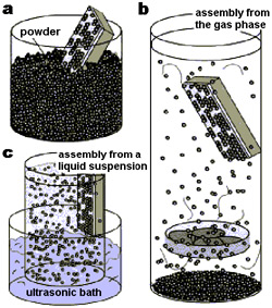
A kind of xerographic printing process for nanoparticles has been developed by Heiko Jacobs and colleagues at the University of Minnesota1. They have deposited nanoparticles in lines just 800 nm wide by using electrostatic forces to control where the particles sit. This is just like the way in which pigment particles are laid down to form an image in xerographic photocopying — but the new technique has a resolution two orders of magnitude higher. In standard xerography, the narrowest line achievable is around 100 µm. Jacobs and co-workers admit that at present they are only skirting the upper reaches of the nanoscale. But they think that even higher resolution should be possible with their approach. The process could be useful for fabricating nanostructures such as quantum-dot arrays or circuits. For example, it might be possible to lay down nanoparticles strictly one-dimensionally this way (that is, in linear arrays), or to use further deposition, growth or sintering steps to join patterns of metal nanoparticles into continuous conductive channels. The attraction is that the entire pattern — the researchers have made patterned areas of up to 1 cm2 — can be deposited in one simple step from either a dry powder, a liquid suspension, or a gas-phase suspension of particles. It is essentially a kind of self-assembly, templated by a pattern of charge laid down on the substrate. The charged regions are defined by a conductive stamp placed in contact with a polymer substrate that forms the 'electret' (the charge-carrying plate used in xerography). The stamp is made from poly(dimethylsiloxane) (PDMS) cast in bas-relief from a silicon-wafer mould. The mould itself is carved out with painstaking high-resolution lithographic methods; but once it is made, a stamp can be used to mass-produce the pattern both cheaply and conveniently. Defining the pattern of electrostatic charge is thus a kind of microcontact printing of the kind now familiar for making low-cost, high-resolution two-dimensional structures. But the printing 'ink' is in this case electrical charge. The PDMS stamp is attached to a copper support plate, and the printing face is covered with a thin film of gold. An electrical contact between the copper plate and this gold film allows the patterned surface to become charged. The stamp is then brought into contact with the substrate, comprised of a thin (80 nm) layer of poly(methylmethacrylate) (PMMA) on a chip of n-doped silicon. When a voltage is applied between the stamp and the silicon layer of the substrate, trapped charges are generated in the PMMA layer, which remain in place when the stamp and substrate are separated. This 'primes' the PMMA electret for particle deposition. This was carried out in three different ways. Jacobs and colleagues dipped the charged chip into a dry powder of particles and then blew away loose particles with a stream of nitrogen. Alternatively, they held the chip in a cloud of particles suspended in a chamber of air or nitrogen by a fan. Or they dipped it into a suspension of particles in a non-polar organic solvent. They investigated three types of particle: commercial carbon-black toner, iron oxide and graphitized carbon, respectively about 25 µm, 500 nm and 100 nm in size. The smallest charge patterns that the researchers have been able
to imprint have features only 150 nm across, as measured by Kelvin probe
force microscopy (a version of the AFM that detects electrostatic charge).
The patterns on which particles were deposited were rather wider, however,
ranging from stripes 60 µm wide for the toner particles to 800 nm
wide for the graphitized carbon particles. In the former case, the researchers
remark that a PMMA film only 80 nm thick was able to hold enough trapped
charge to capture particles over two orders of magnitude larger. Clearly,
this substrate develops a prodigious sticking power.
|
|