Cover Picture: Fabrication of Multicomponent Microsystems by Directed
Three-Dimensional Self-Assembly (Adv. Funct. Mater. 5/2005)
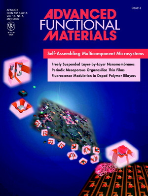 Directed
three-dimensional self-assembly to assemble and package integrated semiconductor
devices is demonstrated by Jacobs and Zheng on p. 732. The self-assembly
process uses geometrical shape recognition to identify different components and
surface-tension between liquid solder and metal-coated areas to form mechanical
and electrical connections.The components (top left) self-assemble in a
turbulent flow (center) and form functional multi-component microsystems (bottom
right) by sequentially adding parts to the assembly solution. The technique
provides, for the first time, a route to enable the realization of
three-dimensional heterogeneous microsystems that contain non-identical parts,
and connecting them electrically.
Directed
three-dimensional self-assembly to assemble and package integrated semiconductor
devices is demonstrated by Jacobs and Zheng on p. 732. The self-assembly
process uses geometrical shape recognition to identify different components and
surface-tension between liquid solder and metal-coated areas to form mechanical
and electrical connections.The components (top left) self-assemble in a
turbulent flow (center) and form functional multi-component microsystems (bottom
right) by sequentially adding parts to the assembly solution. The technique
provides, for the first time, a route to enable the realization of
three-dimensional heterogeneous microsystems that contain non-identical parts,
and connecting them electrically.
We have developed a directed self-assembly process for the fabrication of
three-dimensional (3D) microsystems that contain non-identical parts and a
statistical model that relates the process yield to the process parameters. The
self-assembly process uses geometric-shape recognition to identify different
components, and surface tension between liquid solder and metal-coated areas to
form mechanical and electrical connections. The concept is used to realize
self-packaging microsystems that contain non-identical subunits. To enable the
realization of microsystems that contain more than two non-identical subunits,
sequential self-assembly is introduced, a process that is similar to the
formation of heterodimers, heterotrimers, and higher aggregates found in nature,
chemistry, and chemical biology. The self-assembly of three-component assemblies
is demonstrated by sequentially adding device segments to the assembly solution
including two hundred micrometer-sized light-emitting diodes (LEDs) and
complementary metal oxide semiconductor (CMOS) integrated circuits. Six hundred
AlGaInP/GaAs LED segments self-assembled onto device carriers in two minutes,
without defects, and encapsulation units self-assembled onto the LED-carrier
assemblies to form a 3D circuit path to operate the final device. The
self-assembly process is a well-defined statistical process. The process follows
a first-order, non-linear differential equation. The presented model relates the
progression of the self-assembly and yield with the process parametersˇŞcomponent
population and capture probabilityˇŞthat are defined by the agitation and the
component design.
Read Full Text | Table of Contents
Inside Front Cover: Freely Suspended Layer-by-Layer Nanomembranes: Testing
Micromechanical Properties (Adv. Funct. Mater. 5/2005)
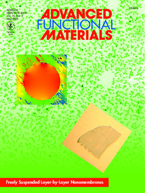 A study
of the micromechanical properties of layer-by-layer nanomembranes composed of a
center layer of gold nanoparticles is reported by Tsukruk and co-workers on
p. 771. The micro- and nanomechanical properties of these membranes are
measured using a combination of resonance-frequency tests, bulging tests, and
point-load nanodeflection experiments. These freely suspended nanomembranes
(right) with an elastic modulus of 5¨C10 GPa are very robust and can
sustain multiple significant deformations (left, image obtained by
B. Rybak and P. Kladitis). They are sensitive to
variations in pressure and therefore have potential applications in pressure and
acoustic sensors.
A study
of the micromechanical properties of layer-by-layer nanomembranes composed of a
center layer of gold nanoparticles is reported by Tsukruk and co-workers on
p. 771. The micro- and nanomechanical properties of these membranes are
measured using a combination of resonance-frequency tests, bulging tests, and
point-load nanodeflection experiments. These freely suspended nanomembranes
(right) with an elastic modulus of 5¨C10 GPa are very robust and can
sustain multiple significant deformations (left, image obtained by
B. Rybak and P. Kladitis). They are sensitive to
variations in pressure and therefore have potential applications in pressure and
acoustic sensors.
Freely suspended nanocomposite layer-by-layer (LbL) nanomembranes composed of
a central layer of gold nanoparticles sandwiched between polyelectrolyte
multilayers are fabricated via spin-assisted LbL assembly. The diameter of the
circular membranes is varied from 150 to 600 &mgr;m and the thickness
is kept within the range of 25¨C70 nm. The micro- and nanomechanical
properties of these membranes are studied using a combination of
resonance-frequency and bulging tests, and point-load nanodeflection
experiments. Our results suggest that these freely suspended nanomembranes, with
a Young's modulus of 5¨C10 GPa are very robust and can sustain multiple
significant deformations. They are very sensitive to minor variations in
pressure, surpassing ordinary semiconductor and metal membranes by three to four
orders of magnitude and therefore have potential applications as pressure and
acoustic microsensors.
Read Full Text | Table of Contents