 |
|
|
|
2005 NSF Research Experience for Teachers (RET) Program |
|
The first two TEM pictures were taken by Dr. Stuart McKernan from the University of Minnesota Characterization Facility. |
|
|
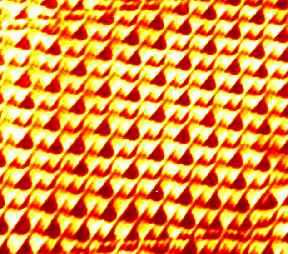
This image is a colorized Transmission Electron Microscope (TEM) image of an array of dislocations on a layered material. The repeating bright orange features displacements of one atomic layer with respect to the others of a few atomic spacings. | |
|
|
|
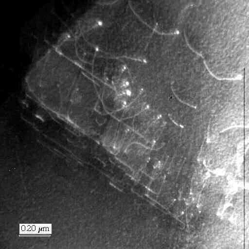
This is another TEM image of Aluminum Nitride (AlN). Notice that the scale on the image is 0.20 microns. |
|
|
|
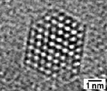
Here is yet another TEM image where atomic structure is very evident. |
|
|
|
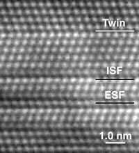
This is a HRTEM (high-resolution TEM) image. The image shows the atomic structure of planar defects in thin-film silicon: a twin defect (in which the upper layers are rotated 180º from the lower layers), an intrinsic stacking fault (ISFin which adjacent layers are shifted slightly), and an extrinsic stacking fault (ESFin which there is an intervening layer between two layers slightly shifted from each other) |
|
|
|
|