
UNIVERSITY OF MINNESOTA
Institute of Technology
Electrical and Computer Engineering Department
Heiko O. Jacobs
Research Interests
Biography
Publications, News,
Patents, Talks
Group Members
Open Positions
Image Gallery
Contact
Nanocourse
Intranet
News, Publications, Patents
Heiko O. Jacobs

Heterogeneous Integration Laboratory (HIL)
Enabling ~ Integration-Across-Length-Scales-&-Material-Boundaries
Through ~ Printing-Transfer-&-Engineered-Self-Assembly
Incorporating ~ Nanoparticle/wires-Microscopic-Dies & Chiplets
News Reports:
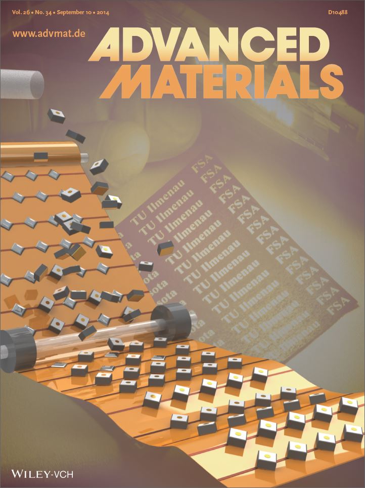
- June 5, 2014, Science Magazine, Editors' Choice, "Faster ways to flexible electronics" highlights Advanced Materials communication on the Realization of Rubber-like Lighting Module using Roll-to-Roll Self-Assembly.
- July 16, 2014, The German Welt der Physik, Spotlights research at the Technische Universität Ilmenau and University of Minnesota in an Article "Lichtpaneele fertigen sich wie von selbst".
- July 10, 2014, Nanowerk, Spotlights research at the Technische Universität Ilmenau and University of Minnesota in an Article "Self-assembly machine - a vision for the future of manufacturing".
- July 4, 2014, The German Physics Portal and the Magazine Optik & Photonik, Highlights research at the Technische Universität Ilmenau and University of Minnesota in an Article "Makroelektronik: Schneller produzieren ohne Roboter".
- July 4, 2014, Advanced Materials Cover, A recent publication of the research team has been selected by the editors of Advanced Materials to be featured on the inside Cover.
- May 25, 2011, Nature Materials, "Mosaic Masters" highlights R. Knuesel and H.O. Jacobs' Advanced Materials communication on Self-Tiling.
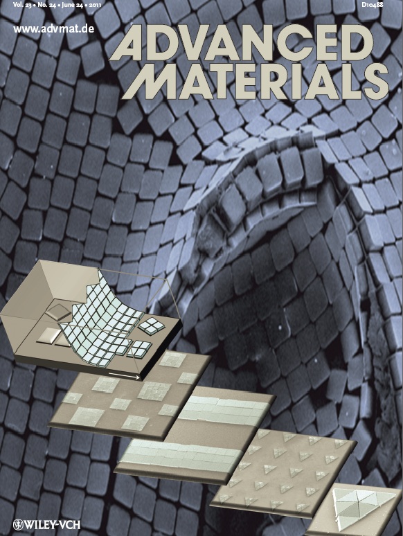
- June 24, 2011, Advanced Materials Cover, Self-Tiling Monocrystalline Silicon; a Process to Produce Electrically Connected Domains of Si and Microconcentrator Solar Cell Modules on Plastic Supports.
- January 14, 2010, Science Magazine, "Shrinkage," featuring UMN research on printable electronics in their January science shot series.
- January 14, 2010, Futura Techno, A French technology news outlet highlights Zheng and Jacobs research on Self-Packaging: "Les puces Èlectroniques pourraient se fabriquer toutes seals" publication.
- January 13-31, 2010, Numerous news outlets (BBC, Ars Technica, Herald, Popular Science, DiscoverMag, TCE Today, TGdaily, Softpedia, Treeh, Golem, News-in-Tech, Printed Electronics World, Green Diary, Engadget, Your Renewable News, Power & Energy, The Green Optimistic, Solar, Ethiopian Review, Energetika, Newstrack India, Physorg, Elektroniktidningen, Rozhlas, Inovacao Tecnologica, Telepolis and many more) report on a recent PNAS article describing a fluidic self-assembly process forming a flexible solar cells.
- January 13, 2010, Golem, A german technology news outlet highlights UMN research in "Solarzelle aus dem Öl-Wasser-Bad" article.
- January 13, 2010, PNAS, The Proceedings of the National Academy of Science flags and highlights R. Knuesel and H.O. Jacobs research article on self-assembling electronics and photovoltaics to be of interest to the broader community and media.
- January 12, 2010, BBC News, Interviews Jacobs and releases a news segment "Solar cells made through oil-and-water 'self-assembly'" that day.
- January 12, 2010, Popular Science, Salad Science: Devices Self-Assemble Using Oil-Water Repulsion.
- January 12, 2010, Ars Technica, Interviews Jacobs and releases the news segment "Self-assembling solar arrays as easy as mixing oil and water" that day.
- January 12, 2010, DISCOVER Magazine Blog, Self-Assembling Solar Panels Use the Vinaigrette Principle.
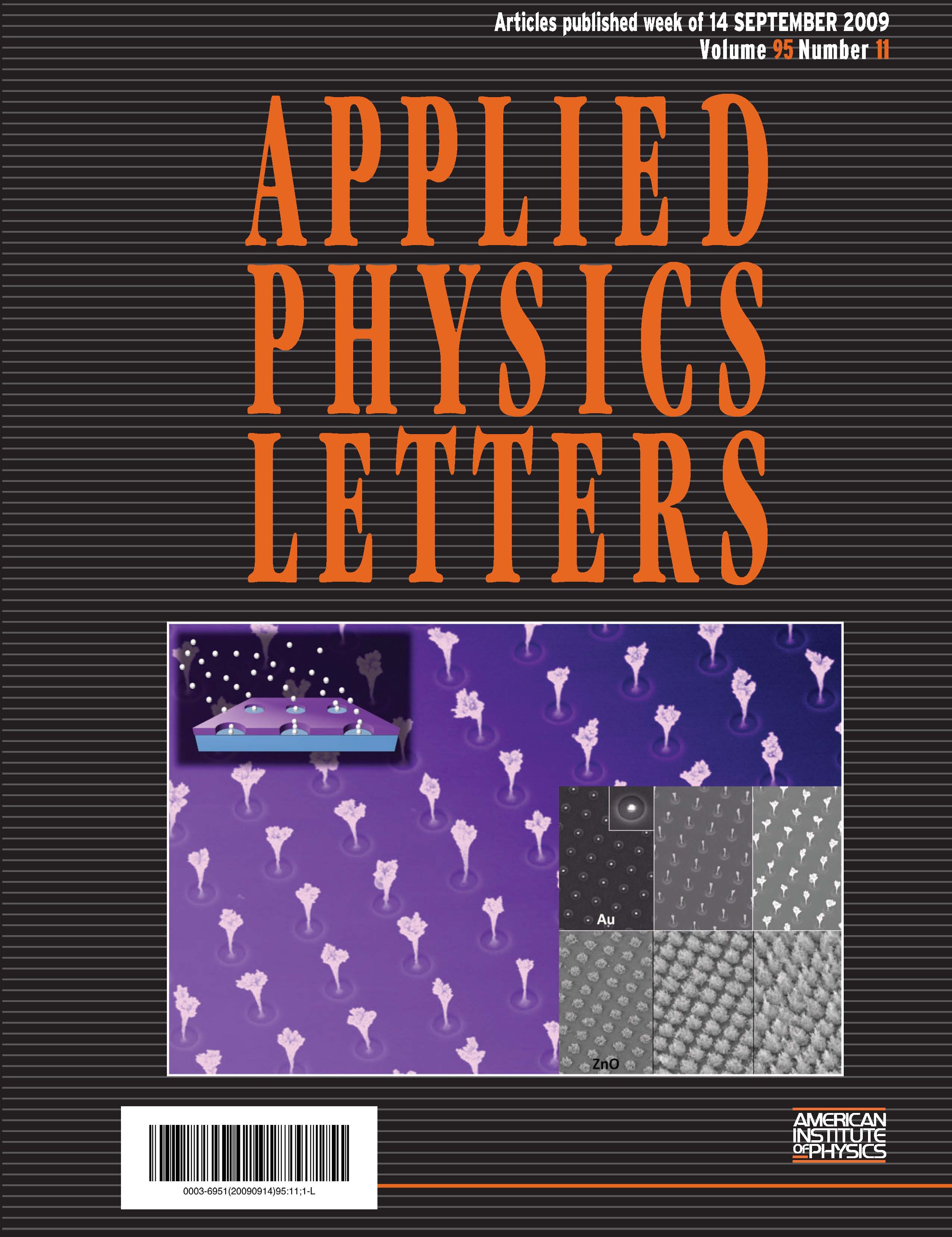
- September 18, 2009, Applied Physics Letters Cover, Continuous Nanoparticle Generation and Assembly by Atmospheric Pressure Arc Discharge.
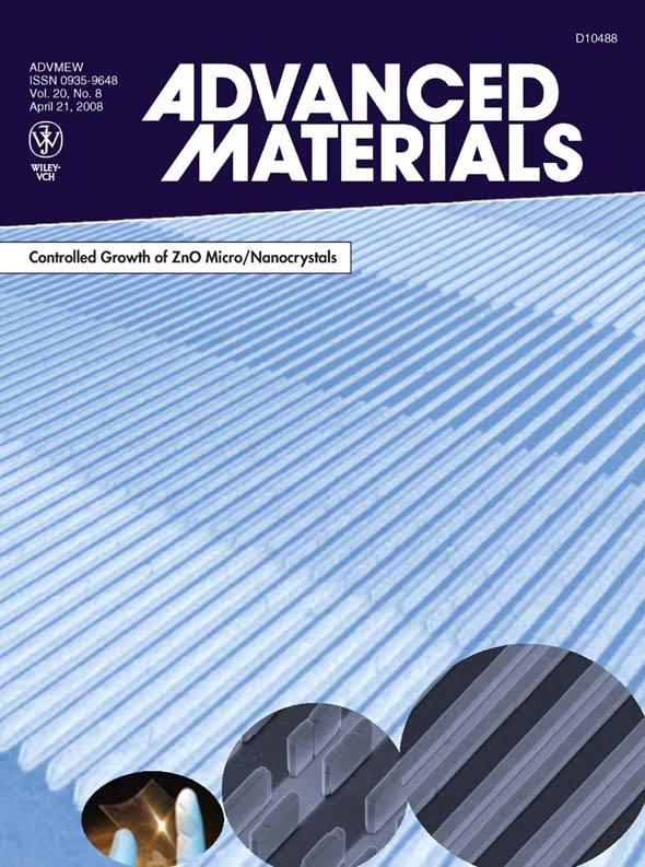
- June 16, 2008, Photonics Spectra, Controlled Growth of ZnO Microcrystals Achieved.
- June 11, 2008, Nature Photonics, Under Control.
- May 16, 2008, Materials Views, ZnO Micro/Nanocrystal Growth.
- April 21, 2008, Advanced Materials Inside Cover, Controlled Growth of ZnO Micro/Nanocrystals.
- January 27, 2006, Graduate Student Chad Barry wins Nanoparticle Industry Innovation Award.
- November 22, 2006, Graduate Student Chad Barry Receives MRS Student Research Gold Award - Directed Assembly of Nanomaterials. [More]
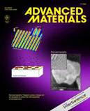
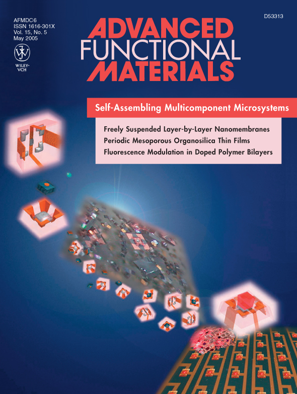
- May 1, 2005, Advanced Functional Materials Cover, Fabrication of Multicomponent Microsystems.
- September 25, 2004, Science News, Bartending lessons for microassembly. [More]
- September 6, 2004, The Dallas Morning news, Self-Assembly Principle Offers Eseful Devices.
- October 28, 2003, Nanotechweb.org, Nanoxerography sets the pattern.
- October 21, 2003, NanoBusiness Alliance, In The Spotlight.
- October 13, 2003, MIT Technology Review, Process Prints Nanoparticles.
- September 26, 2003, Nanoforum - European Nanotechnology Gateway, Small Copiers, Editors' Choice.
- September 26, 2003, Science Magazine, Small Copiers. [More]
- February 2, 2003, National Science Foundation, CAREER Award.
- November 27, 2002, Nature Publishing Group, Nanoscale Photocopies.
- November 25, 2002, Materials News from MRS, Nanoxerography: Creating nanoscale photocopies.
- November 4, 2002, Adanced Materials Cover, Approaching Nanoxerography.
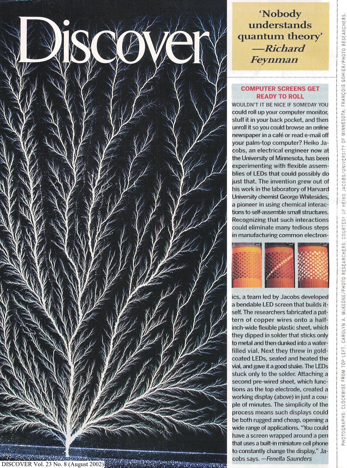
- August 1, 2002, Discover Magazine, Computer Screens Get Ready to Roll.
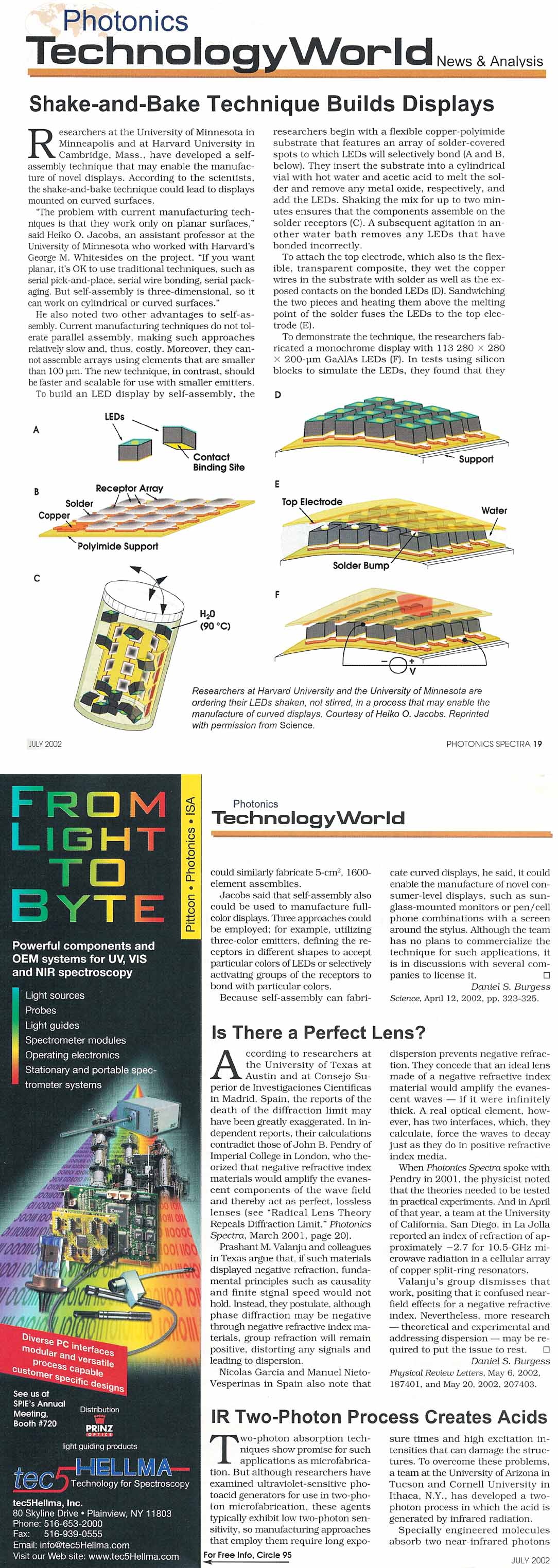
- July 1, 2002, Photonics Spectra, Shake-and-Bend Techniques Builds Displays.
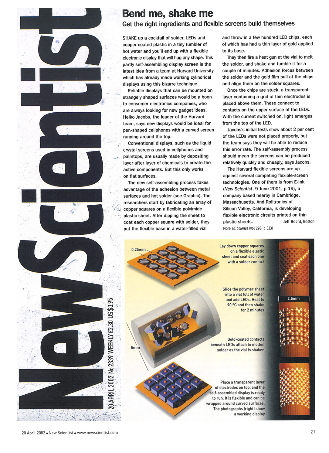
- April 20, 2002, NewScientist, Bend me, shake me.
- April 17/24, 2002, Technology Research News, Add ingredients, shake and serve.
- April 15, 2002, Chemical & Engineering News, SELF-ASSEMBLY REQUIRED.
- March 21, 2001, Technology Research News, Rubber stamp leaves electronic mark.
- July/August, 2001, MIT Technology Review, Gold Standard.
Publications by Topic:
View by: All, Journal, Proceedings, Topic, Patents & Posters/Presentations
Nanomaterials, Nanoparticles, Nanowires, Patterned Growth, Printing & Applications
Microsopic Dies / Microsystems / Patterned Assembly
Top Down Patterning Processes & Scanning Probes & MEMS (10 years ago)
Nanomaterials, Nanoparticles, Nanowires, Patterned Growth, Printing & Applications
- Jun Fang, Se-Chul Park, Leslie Schlag, Thomas Stauden, Jörg Pezoldt, and Heiko O. Jacobs,
"Localized Collection of Airborne Analytes: A Transport Driven Approach to Improve the Response Time of Existing Gas Sensor Designs," Advanced Functional Materials 24(24), 3706-3714
(2014).

- En-Chiang Lin , Jun Fang , Se-Chul Park , Thomas Stauden , Joerg Pezoldt , and Heiko O. Jacobs,
"Effective Collection and Detection of Airborne Species Using SERS-Based Detection and Localized Electrodynamic Precipitation," Advanced Materials 25(26), 3554–3559
(2013).
- En-Chiang Lin, Jun Fang, Se-Chul Park, Forrest W. Johnson, and Heiko O. Jacobs,
"Effective Localized Collection and Identification of Airborne Species Through Electrodynamic Precipitation and SERS-Based Detection," Nature Communications 4-1636
(2013).
- Jesse J. Cole, Chad R. Barry, Robert J. Knuesel, Xinyu Wang, and Heiko O. Jacobs,
"Nanocontact Electrification: Patterned Surface Charges Affecting Adhesion, Transfer, and Printing," Langmuir 27(11), 7321-7329
(2011).
- Jesse J. Cole, En-Chiang Lin, Forrest Johnson, Jun Fang, and Heiko O. Jacobs,
"Nanowire Integration Processes to Gain Control over Location, Dimension, and Orientation," Proc. NSF CMMI Grantees Conference, Atlanta, GA
(2011).
- Jesse J. Cole, En-Chiang Lin, Jun Fang, Forrest Johnson, and Heiko O. Jacobs,
"Gas Phase Nanoxerographic Nanomaterial Integration," Proc. NSF CMMI Grantees Conference, Atlanta, GA
(2011).
- Jesse J. Cole, Chad R. Barry, Xinyu Wang and Heiko O. Jacobs,
"Nanocontact Electrification Through Forced Delamination of Dielectric Interfaces," ACS Nano 4(12), 7492-7498
(2010).
- En-Chiang Lin, Jesse J. Cole and Heiko O. Jacobs,
"Gas Phase Electrodeposition: A Programmable Multimaterial Deposition Method for Combinatorial Nanostructured Device Discovery," Nano Letters 10(11), 4494-4500
(2010).
- Jesse J. Cole, En-Chiang Lin, Chad R. Barry and Heiko O. Jacobs,
"Mimicking Electrodeposition in the Gas Phase: A Programmable Concept for Selected-Area Fabrication of Multimaterial Nanostructures," Small 6(10), 1117-1124
(2010).
- Jesse J. Cole, En-Chiang Lin, Chad R. Barry and Heiko O. Jacobs,
"Continuous Nanoparticle Generation and Assembly by Atmospheric Pressure Arc Discharge," Applied Physics Letters 95(11), 113101/1-113101/3
(2009).
(Cover Picture)
- Chris Smith, Jesse Cole, En-Chiang Lin and Heiko O. Jacobs,
"ZnO Nanorod LEDs and Silicon Nanowire Integration," Proc. NSF CMMI Grantees Conference, Honolulu, HI
(2009).
- Jesse J. Cole, En-Chiang Lin, Chad Barry and Heiko O. Jacobs,
"Gas Phase Nanomaterial Integration," Proc. NSF CMMI Grantees Conference, Honolulu, HI
(2009).
- Jesse J. Cole and Heiko O. Jacobs,
"ZnO Patterned Growth and Transfer Gaining Control over Location, Dimension, and Orientation forming UV LEDs and Photovoltaic Cells," Proc. NSF CMMI Grantees Conference, Honolulu, HI
(2009).
- Jesse J. Cole and Heiko O. Jacobs,
"ZnO Microcrystals for Light Emitting Diode and Photovoltaic Applications with Integration on Flexible Substrates," Proc. Materials Research Society Symp. PP Materials and Devices for Flexible and Stretchable Electronics, San Francisco, CA
(2009).
- Jesse J. Cole, Xinyu Wang, Robert J. Knuesel and Heiko O. Jacobs,
"Integration of ZnO Microcrystals with Tailored Dimensions Forming Light Emitting Diodes and UV Photovoltaic Cells," Nano Letters 8(5), 1477-1481
(2008).
- Jesse J. Cole, Xinyu Wang, Robert J. Knuesel and Heiko O. Jacobs,
"Patterned Growth and Transfer of ZnO Micro- and Nanocrystals with Size and Location Control," Advanced Materials 20(8), 1474-1478
(2008).
(Cover Picture)
- Chad Barry, Xinyu Wang, Uwe Kortshagen and Heiko O. Jacobs,
"Gas Phase Nanoparticle Integration," Proc. Materials Research Society Symp. N Printing Methods for Electronics, Photonics and Biomaterials, San Francisco, CA
(2007).
- Chad R. Barry and Heiko O. Jacobs,
"Gas Phase Nanoparticle Integration," Proc. NSTI-Nanotech Conference, Santa Clara, CA
(2007).
- Xinyu Wang, Jesse Cole, Amir M. Dabiran and Heiko O Jacobs,
"Electroluminescence of ZnO Nanowire/p-GaN Heterojunction Light Emitting Diodes," Proc. NSTI-Nanotech Conference, Santa Clara, CA
(2007).
- Xinyu Wang, Jesse Cole, Amir Dabiran and Heiko O. Jacobs,
"ZnO Nanowire/p-GaN Heterojunction LEDs, in Applications of Nanotubes and Nanowires," Proc. Materials Research Society 1018E edited by Phaedon Avouris
(2007).
- Chad R. Barry and Heiko O. Jacobs,
"Fringing Field Directed Assembly of Nanomaterials," Nano Letters 6(12), 2790-2796
(2006).
- Chad R. Barry, Jie Gu and Heiko O. Jacobs,
"Charging Process and Coulomb-Force-Directed Printing of Nanoparticles with Sub-100 nm Lateral Resolution," Nano Letters 5(10), 2078-2084
(2005).
- Aaron M. Welle and Heiko O. Jacobs,
"Printing of Organic and Inorganic Nanomaterials Using Electrospray Ionization and Coulomb-Force-Directed Assembly," Applied Physics Letters 87(26), 263119/1-263119/3
(2005).
- Chad R. Barry, Aaron M. Welle, Jie Gu, Stephen A. Campbell and Heiko O. Jacobs,
"Printing of Nanoparticles with Sub-100nm Resolution," Proc. NSF CMMI Grantees Conference, Scottsdale, AZ
(2005).
- Yongping Ding, Ying Dong, Stephen A. Campbell and Heiko O. Jacobs,
"Field-Effect Transistor Built with a Single Crystal Si Nanoparticle," Proc. NSF CMMI Grantees Conference, Scottsdale, AZ
(2005).
- Chad R. Barry, Aaron M. Welle, Uwe Kortshagen, Stephen A. Campbell and Heiko O. Jacobs, "From Electric Nanocontact Lithography to the Directed Self-Assembly of Nanoparticle Based Devices," Proc. Nanoarchitectonics, Tsukuba, Japan (2005).
- J. Basu, R. Divarkar, J. Deneen, X. Wang, H.O. Jacobs and C.B. Carter,
"Interfaces of ZnO Nanowires Grown on Semiconducting Surfaces," Proc. Microscopy and Microanalysis Conference, Chicago, IL
(2005).
- C. R. Barry, N. Z. Lwin, M.G. Steward and H. O. Jacobs,
"Nanoparticle Assembly by Nanoxerography," Proc. NSF CMMI Grantees Conference, Dallas, TX
(2004).
- C. R. Barry, C. J. Hoon and H. O. Jacobs,
"Approaching Programmable Self-Assembly from Nanoparticle-Based Devices to Integrated Circuits," Proc. Foundations of Nanoscience: Self-Assembled Architectures and Devices (FNANO), Snowbird, UT (Invited)
(2004).
- J. Gu, C. R. Barry and H. O. Jacobs,
"NanoXerography: The Directed Self-Assembly of Nanoparticle Building Blocks onto Charged Based Receptors," Proc. 7th International Conference on Nanostructured Materials, Wiesbaden, Germany
(2004).
- Chad R. Barry, Michael G. Steward, Nyein Z. Lwin and Heiko O. Jacobs,
"Printing Nanoparticles From the Liquid and Gas-Phase Using Nanoxerography," Nanotechnology 14(10), 1057-1063 (Invited Featured Article)
(2003).
- Chad R. Barry, Nyein Z. Lwin, Wei Zheng and Heiko O. Jacobs,
"Printing Nanoparticle Building Blocks From the Gas-Phase Using Nanoxerography," Applied Physics Letters 83(26), 5527-5529
(2003).
(Cover Picture)
- Michael G. Steward, Chad R. Barry, Stephen A. Campbell and Heiko O. Jacobs,
"NanoXerography: The Use of Electrostatic Forces to Pattern Nanoparticles," Proc. NSF CMMI Grantees Conference, Birmingham, AL
(2003).
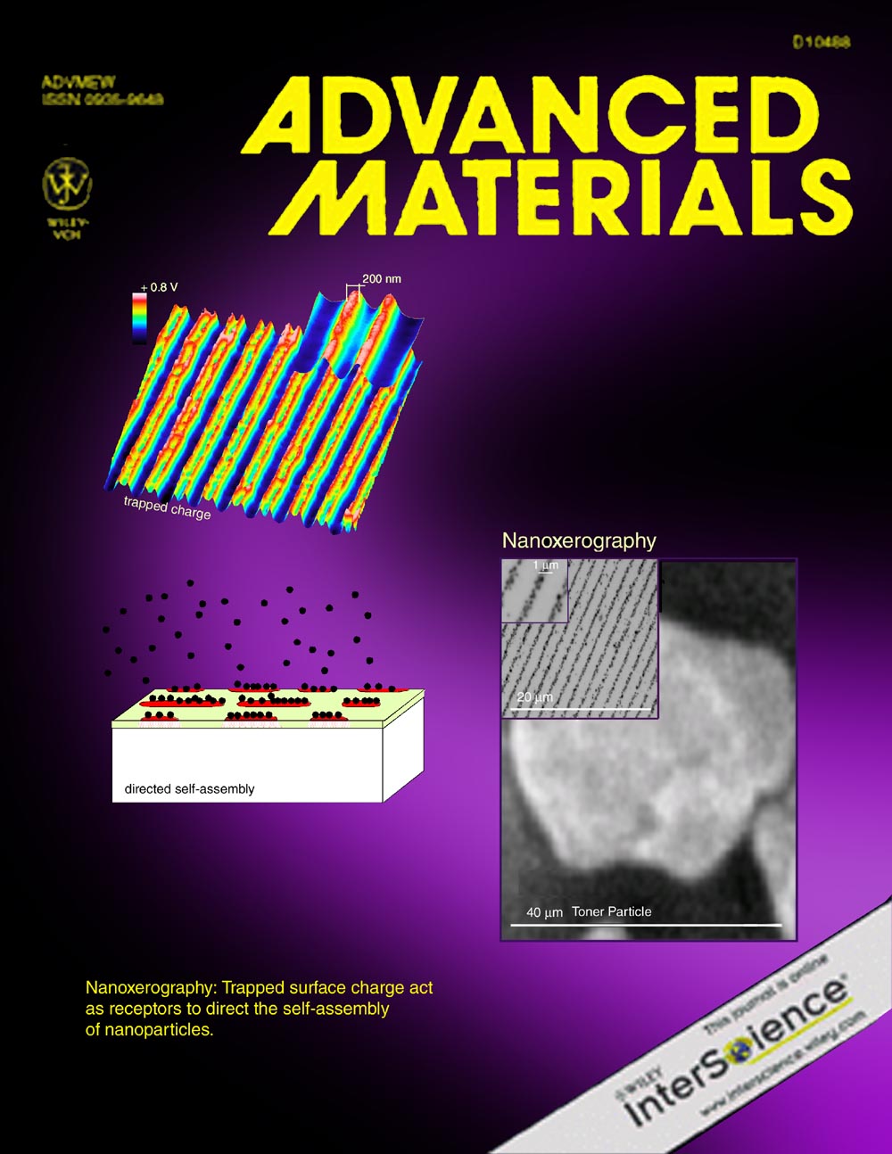
- H. O. Jacobs, S. A. Campbell and M. G. Steward,
"Approaching NanoXerography: The use of Electrostatic Forces to Position Nanoparticles with 100 Nanometer Scale Resolution," Advanced Materials 14(21), 1553-1557
(2002).
(Cover Picture)
Nanomaterials, Nanoparticles, Nanowires, Patterned Growth, Printing & Applications
Microsopic Dies / Microsystems / Patterned Assembly
Top Down Patterning Processes & Scanning Probes & MEMS (10 years ago)
Microscopic Dies / Microsystems / Patterned Assembly
- Se-Chul Park, Shantonu Biswas, Jun Fang, Mahsa Mozafari, Thomas Stauden and Heiko O. Jacobs,
"Millimeter Thin and Rubber-Like Solid-State Lighting Modules Fabricated Using Roll-to-Roll Fluidic Self-Assembly and Lamination," Advanced Materials (DOI:10.1002/adma.201500839)
(2015).
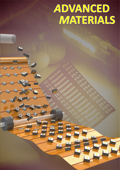
- Se-Chul Park, Jun Fang, Shantonu Biswas, Mahsa Mozafari, Thomas Stauden and Heiko O. Jacobs,
"A First Implementation of an Automated Reel-to-Reel Fluidic Self-Assembly Machine," Advanced Materials 26 (34), 5942-5949
(2014).
(Cover Picture)
- Robert J. Knuesel, Sechul Park, Wei Zheng, and Heiko O. Jacobs,
"Self-assembly and Self-tiling: Integrating Active Dies Across Length Scales on Flexible Substrates," Journal of Microelectromechanical Systems 21(1), 58-99
(2011).
- Robert J. Knuesel and Heiko O. Jacobs,
"Self-Tiling Monocrystalline Silicon; A Process to Produce Electrically Connected Domains of Si and Microconcentrator Solar Cell Modules on Plastic Supports," Advanced Materials 23(24), 2727-2733
(2011).
(Cover Picture)
- Robert J. Knuesel, Se-Chul Park, and Heiko O. Jacobs,
"Self-Packaging and Self-Mounting of Miniaturized Semiconductor Dies Across Length Scales and 3D Topologies," Proc. Foundations of Nanoscience: Self-Assembled Architectures and Devices (FNANO10), Snowbird, Utah
(2010).
- Robert J. Knuesel and Heiko O. Jacobs,
"Self-Assembly of Microscopic Chiplets at a Liquid-Liquid-Solid Interface Forming a Flexible Segmented Monocrystalline Solar Cell," Proceedings of the National Academy of Sciences, USA 107(3), 993-998
(2010).
- Robert J. Knuesel, Wei Zheng, Jaehoon Chung, Se-Chul Park, Michael J. Motala, and Heiko O. Jacobs,
"Directed Assembly: Integration of Heterogeneous Systems Across Length Scales and Material Boundaries," Proc. NSF ECCS Grantees Conference, Honolulu, HI
(2010).
- Robert J. Knuesel, Se-Chul Park, Michael J. Motala, and Heiko O. Jacobs,
"Scaling Limits of Programmable Fluidic Self-Assembly Forming Electrical Interconnects," Proc. NSF ECCS Grantees Conference, Honolulu, HI
(2010).
- Robert J. Knuesel and Heiko O. Jacobs,
"Fluidic Surface-Tension-Directed Self-Assembly of Miniaturized Semiconductor Dies Across Length Scales and 3D Topologies," Proc. Materials Research Society Symp. BB Material Systems and Processes for Three-Dimensional Micro- and Nanoscale Fabrication and Lithography, San Francisco, CA
(2009).
- Jesse J. Cole, Xinyu Wang, Robert J. Knuesel and Heiko O. Jacobs,
"Patterned Growth and Transfer of ZnO Micro- and Nanocrystals with Size and Location Control," Advanced Materials 20(8), 1474-1478
(2008).
(Cover Picture)
- Robert Knuesel, Shameek Bose, Wei Zheng and Heiko O. Jacobs,
"Angular Orientation-Specific Directed Self-assembly and Integration of Ultra Small Dies," Proc. NSTI-Nanotech Conference, Santa Clara, CA
(2007).
- Robert Knuesel, Shameek Bose, Wei Zheng and Heiko O. Jacobs,
"Engineered Solder-Directed Self-Assembly Across Length Scales, in Materials, Processes, Integration, and Reliability in Advanced Interconnects for Micro- and Nano-Electronics," Proc. Materials Research Society 990 edited by Robert Miller and Dorel Toma
(2007).
- Wei Zheng, Jae-hoon Chung and Heiko O. Jacobs,
"Fluidic Heterogeneous Microsystems Assembly and Packaging," Journal of Microelectromechanical Systems 15(4), 864-870
(2006).
- Jae-hoon Chung, Wei Zheng, Thomas J. Hatch and Heiko O. Jacobs,
"Programmable Reconfigurable Self-Assembly: Parallel Heterogeneous Integration of Chip-Scale Components on Planar and Nonplanar Surfaces," Journal of Microelectromechanical Systems 15(3), 457-464
(2006).
- Wei Zheng and Heiko O. Jacobs,
"Self-Assembly Process To Assemble and Connect Semiconductor Dies On Surfaces with Single Angular Orientation and Contact Pad Registration," Advanced Materials 18(11), 1387-1392
(2006).
- Wei Zheng and Heiko O. Jacobs,
"Fabrication of Multicomponent Microsystems by Directed Three-Dimensional Self-Assembly," Advanced Functional Materials 15(5), 732-738
(2005).
(Cover Picture)
- W. Zheng, J.H. Chung and H. O. Jacobs,
"Non-Robotic Fabrication of Packaged Microsystems By Shape-And-Solder directed Self-Assembly," Proc. 18th IEEE International Conference on Micro Electro Mechanical Systems (MEMS 2005), Miami Beach, FL
(2005).
- J.H. Chung, W. Zheng and H. O. Jacobs,
"Programmable Reconfigurable Self-Assembly: Approaching The Parallel Heterogeneous Integration on Flexible Substrates," Proc. 18th IEEE International Conference on Micro Electro Mechanical Systems (MEMS 2005), Miami Beach, FL
(2005).
- Wei Zheng, Philippe Buhlmann and Heiko O. Jacobs,
"Sequential Shape-and-Solder-Directed Self-Assembly of Functional Microsystems," Proceedings of the National Academy of Sciences, USA 101(35), 12814-12817
(2004).
- Wei Zheng and Heiko O. Jacobs,
"Shape-and-Solder-Directed Self-Assembly to Package Semiconductor Device Segments," Applied Physics Letters 85(16), 3635-3637
(2004).
- C. R. Barry, C. J. Hoon and H. O. Jacobs,
"Approaching Programmable Self-Assembly from Nanoparticle-Based Devices to Integrated Circuits," Proc. Foundations of Nanoscience: Self-Assembled Architectures and Devices (FNANO), Snowbird, UT (Invited)
(2004).
- M. Boncheva, D.H. Gracias, H.O. Jacobs and G.M. Whitesides,
"Biomimetic Self-Assembly of a Functional Asymmetrical Electronic Device," Proceedings of the National Academy of Sciences, USA 99(8), 4937-4940
(2002).
- H.O. Jacobs, A.R. Tao, A. Schwartz, D.H. Gracias and G.M. Whitesides,
"Fabrication of a Cylindrical Display by Patterned Assembly," Science 296(5566), 323-325
(2002).
Nanomaterials, Nanoparticles, Nanowires, Patterned Growth, Printing & Applications
Microsopic Dies / Microsystems / Patterned Assembly
Top Down Patterning Processes & Scanning Probes & MEMS (10 years ago)
Top Down Patterning
- M. L. Chabinyc, X. Chen, R. E. Holmlin, H. O. Jacobs, H. Skulason, C. D. Frisbie, V. Mujica, M. A. Ratner, M. A. Rampi and G. M. Whitesides,
"Molecular Rectification in a Metal-Insulator-Metal Junction Based on Self-Assembled Monolayers," Journal of the American Chemical Society 124(39), 11730-11736
(2002).
- F. Robin, H. Jacobs, O. Homan, A. Stemmer and W. Bachtold, "Investigation of the Cleaved Surface of a p-i-n Laser Using Kelvin Probe Force Microscopy and Two-Dimensional Physical Simulations," Applied Physics Letters 76(20), 2907-2909 (2000).
- H. O. Jacobs and A. Stemmer,
"Measuring and Modifying the Electric Surface Potential Distribution on a Nanometre Scale: a Powerful Tool in Science and Technology," Surface and Interface Analysis 27(5-6), 361-367
(1999).
- H. O. Jacobs, H. F. Knapp and A. Stemmer,
"Practical Aspects of Kevin Probe Force Microscopy," Review of Scientific Instruments 70(3), 1756-1760
(1999).
- H. O. Jacobs, P. Leuchtmann, O. J. Homan and A. Stemmer,
"Resolution and Contrast in Kelvin Probe Force Microscopy," Journal of Applied Physics 84(3), 1168-1173
(1998).
- H. O. Jacobs, H. F. Knapp, S. Müller and A. Stemmer,
"Surface Potential Mapping: A Qualitative Material Contrast in SPM," Ultramicroscopy 69(1), 39-49
(1997).
- A. Stemmer, H. O. Jacobs and H. F. Knapp,
"Approaching the Nanoworld," Proc. SPIE Microrobotics: Components and Applications 2906, 80-85
(1996).
Nanomaterials, Nanoparticles, Nanowires, Patterned Growth, Printing & Applications
Microsopic Dies / Microsystems / Patterned Assembly
Top Down Patterning Processes & Scanning Probes & MEMS (10 years ago)
Scanning Probes, Metrology
- Chad R. Barry, Aaron M. Welle, Uwe Kortshagen, Stephen A. Campbell and Heiko O. Jacobs, "From Electric Nanocontact Lithography to the Directed Self-Assembly of Nanoparticle Based Devices," Proc. Nanoarchitectonics, Tsukuba, Japan (2005).
- J. Gu, C. R. Barry and H. O. Jacobs,
"NanoXerography: The Directed Self-Assembly of Nanoparticle Building Blocks onto Charged Based Receptors," Proc. 7th International Conference on Nanostructured Materials, Wiesbaden, Germany
(2004).
- H. O. Jacobs,
"Patterning of Electrons and Holes for Data Storage and High Resolution Charge Based Printing," Proc. 7th International Conference on Nanometer-scale Science and Technology, NANO-7/ECOSS-21 A2183, Malmo, Sweden
(2002).
- J. Ch. Love, D. B. Wolfe, H. O. Jacobs and G. M. Whitesides,
"Microscope Projection Photolithography for Rapid Prototyping of Masters with Micron-Scale Features for Use in Soft Lithography," Langmuir 17(19), 6005-6012
(2001).
- H. O. Jacobs and G. M. Whitesides,
"Submicrometer Patterning of Charge in Thin-Film Electrets," Science 291(5509), 1763-1766
(2001).
- H. O. Jacobs and A. Stemmer,
"Measuring and Modifying the Electric Surface Potential Distribution on a Nanometre Scale: a Powerful Tool in Science and Technology," Surface and Interface Analysis 27(5-6), 361-367
(1999).
Nanomaterials, Nanoparticles, Nanowires, Patterned Growth, Printing & Applications
Microsopic Dies / Microsystems / Patterned Assembly
Top Down Patterning Processes & Scanning Probes & MEMS (10 years ago)
Traditional MEMS (10 years ago)
- F. Mayer, A. Häberli, H. Jacobs, G. Ofner, O. Paul and H. Baltes,
"Single-Chip CMOS Anemometer," Proc. IEEE International Electron Device Meeting 895-898
(1997).
- F. Mayer, M. Hintermann, H. Jacobs, O. Paul and H. Baltes,
"Thermoelectric CMOS Anemometers," Proc. SPIE Micromachined devices and Components II 2882, 236-246
(1996).